What’s the reason for copper on the corner holes? I presume it can’t be relied upon for an electrical connection between the chassis, fastener and panel because it has soldermask over it.
Looking at my supplied banana plug front panel, the corner holes are not PTH - please confirm.
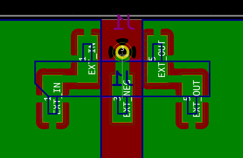
Is the location of the via from pin 3 to the front copper pour important, or just get it roughly in the right place.
Hi @simonmerrett: Happy to help. You are one of the first people (other than me) to design a front panel. Your questions will help us improve the documentation and process for everyone!
Just to help with wear, but you don’t need copper. The chassis is referenced to USB ground, and the sensor IN and sensor OUT are isolated. You do need to maintain a minimum 1 mm clearance from the screws to any IN or OUT signal. Larger clearance helps with noise immunity, which explains the rounded oval copper shape of the existing front panels.
The existing modules did not use PTH, but you can. Again, no reason for or against. The light pipe hole is not plated, so making them plated will not save a fab step. However, you could potentially plate both if cost measured in pennies becomes a concern.
Not important. You do need to plan sufficient copper (and vias if needed) for the current into pins 1-2 and 4-5. Joulescope supports 3A max with 10A bursts, so you need to consider plane resistance if your front panel supports that full range. Pin 3 is high impedance (< 10 nA current), so whatever.
Very helpful, thanks. I admit I have found the dimensions harder to generate layout from. Kicad bases footprints on a 0,0 coordinate and so the centre of the panel would be the easiest datum to work from. I’m fine with the calculator though!
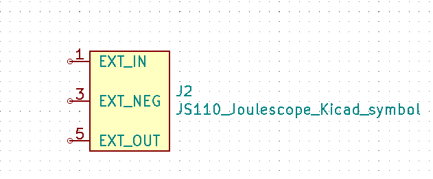
I think I have made some progress (had to pause for a barbecue!). I have made a JS110 symbol:
Pins 2 and 4 are not visible and are automatically connected to pins 1 and 5 respectively.
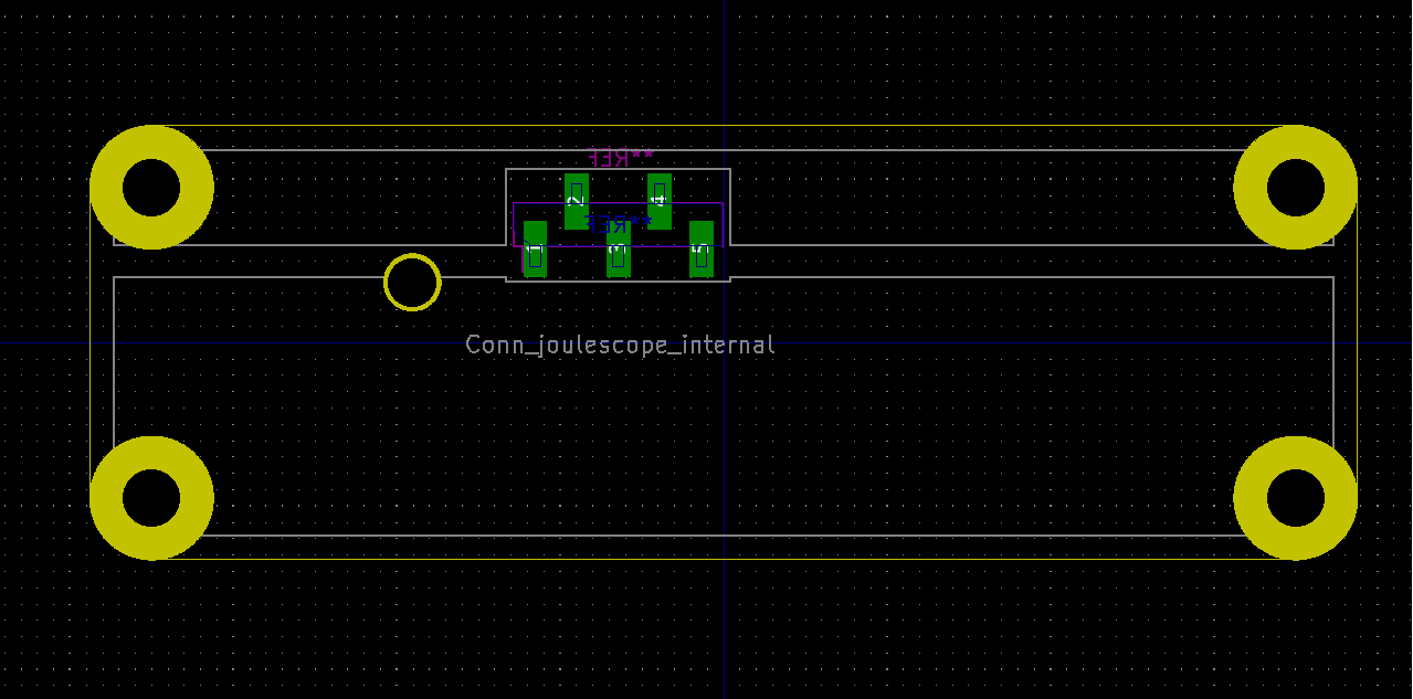
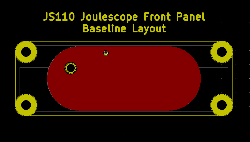
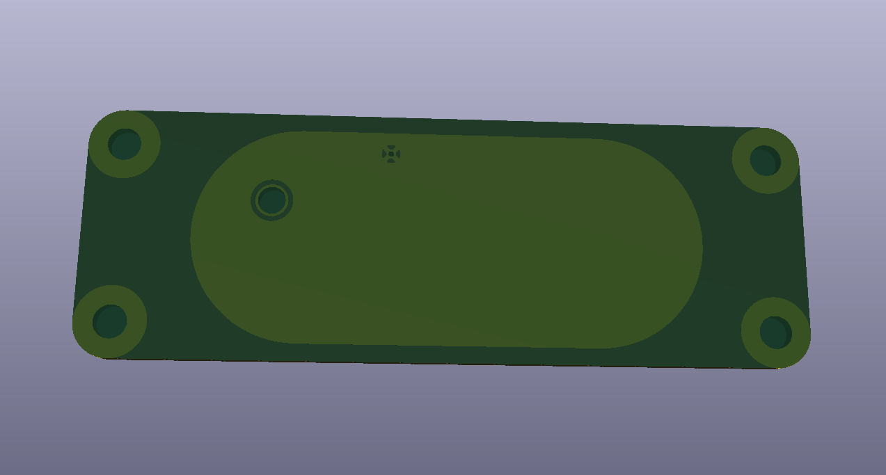
I have also made the front panel as a single footprint, incorporating:
PCB edge/outline in the Edge.Cuts layer
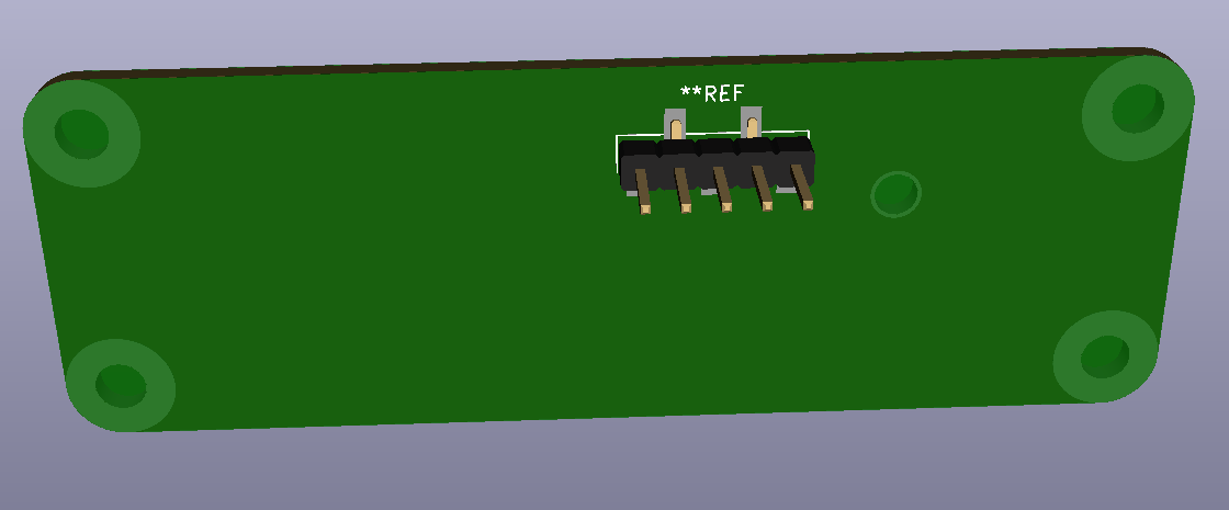
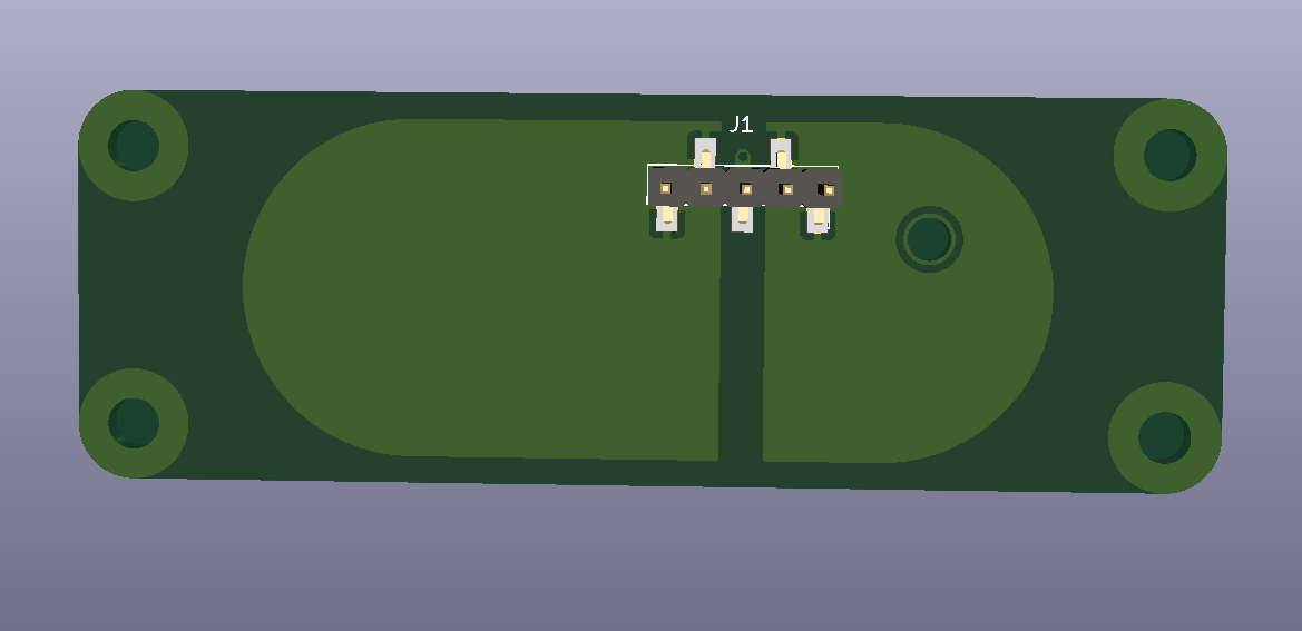
SAMTEC connector footprint (larger than the standard 5 pin SMD pads in the normal Kicad PinHeader footprint library - I tried to copy the dimensions in the Eagle .brd) on the back side
PTH for the light pipe - converted 0.115" to 2.921mm so rounded up to 2.93 (as if that’s a drill size!)
PTH for the four mounting screw holes.
All PTH are covered in soldermask
Back side edge, middle and connector keepouts implemented as a continuous area enclosed by edge lines on B.CrtYd layer in Kicad. This appears to work in the DRC if another part’s courtyard overlaps and it is on the back side only.
The 3D renderer accepts the edge cuts but doesn’t recognise the holes in the soldermask for the PTH because I unticked the F.Mask and B.Mask in the pad settings, in order to cover them up with solder mask.
On the back face of the banana jack front panel (Rev 6) that I have, you have put a silkscreen pair of solid lines on the edge of your lateral keepout. Do you want this replicated in the baseline Kicad footprint? A Kicad user is free to add or remove this locally, on each board they employ the footprint on, using the footprint editor.
Do you want me to use e.g. a fabrication layer to outline where the rounded copper pour segments would go? Or do you want me to put the copper pour segments in? In either case, please give me dimensions for those features.
Pins 1 & 2 and 4 & 5 are always common/connected, so do you want me to add copper to the SAMTEC connector footprint to make sure they are electrically connected within the footprint? The Kicad ratsnest is asking to connect them to each other (separate nets of course) when I add it to a board.
Nomenclature: I’m already fragmenting with e.g. Conn_joulescope_internal, Joulescope_FP_baseline, JS110_Joulescope_Kicad_Symbol etc. We need to name the schematic symbol file and the footprint file, as well as have some identification text within each file. Any thoughts/preferences? I’m aware that you’re actually doing proper version control, so I’d like to help, rather than hinder, with that.
How are we going to QA this part? Are you going to download Kicad and check yourself?Dimensioning has to be done in the board design, not the footprint editor, but the dimensions won’t lock onto e.g. the centre of PTH in a footprint. I suggest avoiding the dimensioning and opening the footprint in the footprint editor, then looking at the coordinates and sizes of each footprint element in their properties (a right-click job).
I put these on to keep myself from making silly mistakes. A backside keepout is probably enough, but I am paranoid I don’t know Kicad yet, so do what you think is right.
Starting with a default copper pour is nice. Check out the USB front panel gerbers. No need to be exact, either.
Up to you! My boards have full pour with no thermals to support the current. This requirement makes the front panel PCBs a pain to assemble…
My opinion is to keep the names similar and rely on the filename extensions where possible.
Since I don’t know Kicad yet, I would just check the gerbers against another front panel design to confirm placement. I am on vacation until Aug 10, so my time is limited in checking until then.
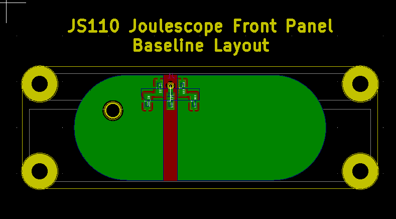
The ground pours on front and back, respectively connected to the relevant pins
I can’t seem to stop the ratsnest from thinking the via and Pin 3 smd pad aren’t connected - but I think they are (one to check on the Gerbers during QA). If any Kicad ninjas know how to stop this, please explain how. Adding a copper filled polygon between Pins 1 & 2 and Pins 4 & 5 seems to silence the ratsnest between them
I have added B.Fab and F.Fab unfilled polygons in the footprint file to show where the ground pours could go. I roughly copied the Eagle .brd pour boundaries. I think I have differed slightly though because I avoided the perimeter keepout on the rear and thought it best to match that on the front too.
Because we want ground pours to automatically adjust to any other nets we add to the PCB, I have not been able to implement the ground pours in the footprint. I have had to add them in the .kicad_pcb file as separate filled zones.
Looking good! To support the full Joulescope current range (3A with 10A bursts) with minimal voltage drop, you will likely need to remove the thermals on pins 1, 2, 4, and 5. Thermals on the pin 3 via are fine since it is very high impedance.
Thermals on the IN and OUT connectors are usually not possible for the same reason. This makes assembly a pain, but what is needed.
I just checked using Gerbv. The outline, corner hole, and light pipe all look good. I noticed a small difference with the soldermask for the 5x1 connector. I checked the Eagle design files, and the component centroid is 32.45 x 20.615 mm. The drawing says 32.45 x 20.61 (close enough).
Looks good, and definitely worth submitting a PR. Place your design under kicad/fp_baseline/. Please also include a CHANGELOG.md file. If you want, also include a README.md file with any instructions for how to best use your KiCAD design, and please give yourself credit in the README or in the design itself.
Great, and you’re welcome. Does this merit (hah!) a mention in the announcements category, so that when this thread is long buried it might be a more natural place to find the info?