I think I have made some progress (had to pause for a barbecue!). I have made a JS110 symbol: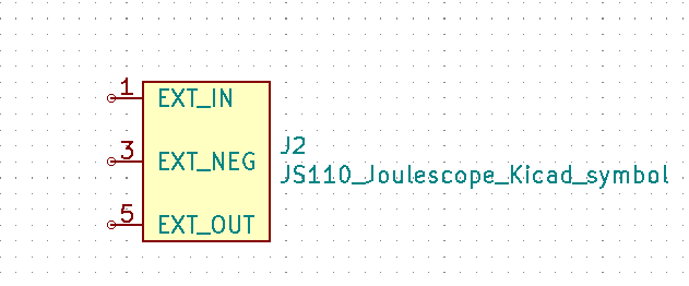
Pins 2 and 4 are not visible and are automatically connected to pins 1 and 5 respectively.
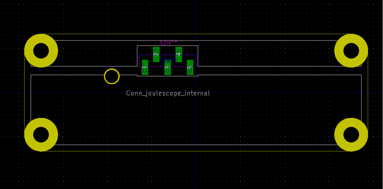
I have also made the front panel as a single footprint, incorporating:
- PCB edge/outline in the Edge.Cuts layer
- SAMTEC connector footprint (larger than the standard 5 pin SMD pads in the normal Kicad PinHeader footprint library - I tried to copy the dimensions in the Eagle .brd) on the back side
- PTH for the light pipe - converted 0.115" to 2.921mm so rounded up to 2.93 (as if that’s a drill size!)
- PTH for the four mounting screw holes.
- All PTH are covered in soldermask
- Back side edge, middle and connector keepouts implemented as a continuous area enclosed by edge lines on B.CrtYd layer in Kicad. This appears to work in the DRC if another part’s courtyard overlaps and it is on the back side only.
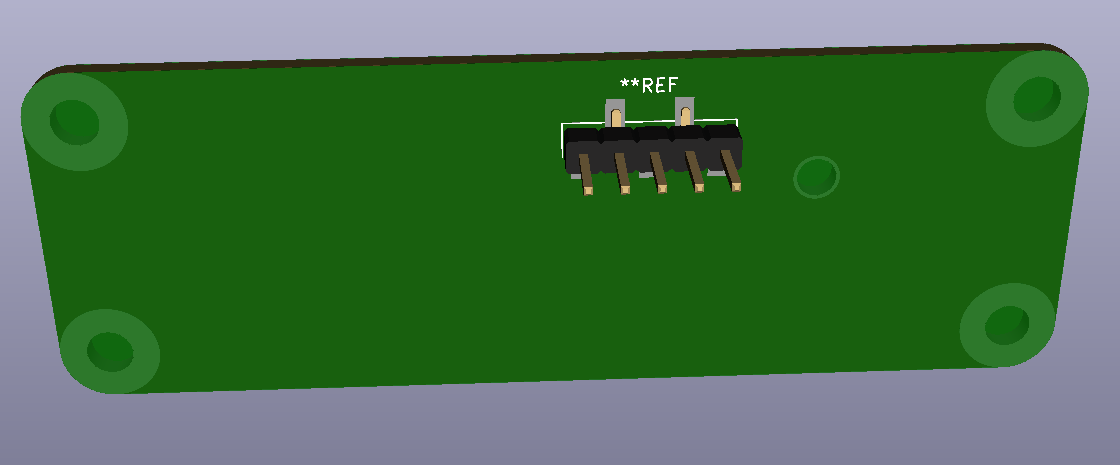
The 3D renderer accepts the edge cuts but doesn’t recognise the holes in the soldermask for the PTH because I unticked the F.Mask and B.Mask in the pad settings, in order to cover them up with solder mask.
More questions:
- On the back face of the banana jack front panel (Rev 6) that I have, you have put a silkscreen pair of solid lines on the edge of your lateral keepout. Do you want this replicated in the baseline Kicad footprint? A Kicad user is free to add or remove this locally, on each board they employ the footprint on, using the footprint editor.
- Do you want me to use e.g. a fabrication layer to outline where the rounded copper pour segments would go? Or do you want me to put the copper pour segments in? In either case, please give me dimensions for those features.
- Pins 1 & 2 and 4 & 5 are always common/connected, so do you want me to add copper to the SAMTEC connector footprint to make sure they are electrically connected within the footprint? The Kicad ratsnest is asking to connect them to each other (separate nets of course) when I add it to a board.
- Nomenclature: I’m already fragmenting with e.g. Conn_joulescope_internal, Joulescope_FP_baseline, JS110_Joulescope_Kicad_Symbol etc. We need to name the schematic symbol file and the footprint file, as well as have some identification text within each file. Any thoughts/preferences? I’m aware that you’re actually doing proper version control, so I’d like to help, rather than hinder, with that.
- How are we going to QA this part? Are you going to download Kicad and check yourself?Dimensioning has to be done in the board design, not the footprint editor, but the dimensions won’t lock onto e.g. the centre of PTH in a footprint. I suggest avoiding the dimensioning and opening the footprint in the footprint editor, then looking at the coordinates and sizes of each footprint element in their properties (a right-click job).